1. temporary programming, meaning that the design will not survive powering off, and
2. permanently storing (flashing) the design, so it will survive power off.
I will also address the idea of a mega-reset using the DEV_CLRn feature at the bottom of this post.
Disclamer: You are doing all of this at your own risk. I am not responsible for any problem caused by these examples. To prevent problems, check the documentation of your DE0-NANO to see if you have the same type of Programmer and EEPROM chips.
1. Temporary programming
Whenever you compile your design at the Quartus II IDE, you can send the design to the FPGA board via Programmer:1. double click on the Program Device in the table:

2. When the Programmer opens, look for the USB blaster right to the Hardware Setup... button:

3. If you see the "No Hardware" text, click on the Hardware Setup... button. That would open the Hardware Setup dialog:

4. Double click the USB Blaster and Close. The Programmer should look like this:
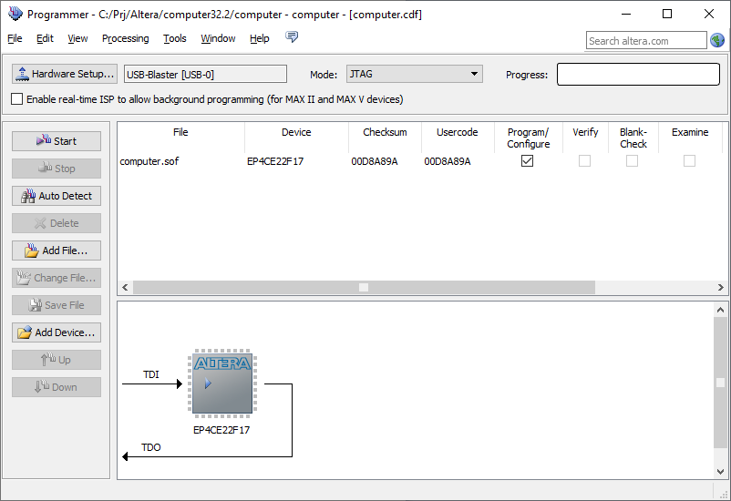
5. Now the USB Blaster is present right to the Hardware Setup... button.
6. Click on the Start button to send the design to the FPGA board.
All this is temporary, meaning that the design will be erased when you power off the board.
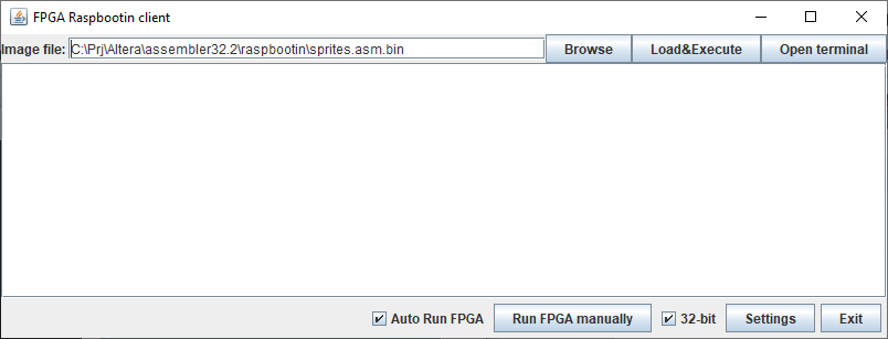
Alternative way of temporary programming
An alternative way of doing this is by executing the following program:C:\altera\13.0\quartus\bin\quartus_pgm.exe
You need to supply that program with the following command line parameters:
-c usb-blaster -m jtag -o P;<path_to_the_SOF_file>
That could be typed like this:
C:\altera\13.0\quartus\bin\quartus_pgm.exe -c usb-blaster -m jtag -o
P;<path_to_the_SOF_file>
I have done that in my FPGARaspbootin program (the Run FPGA manually button, and Auto Run FPGA check box):
2. Permanent programming (flashing)
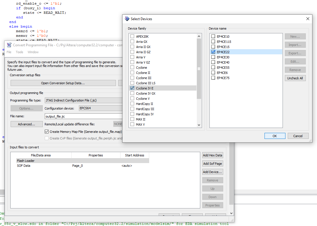
To flash the DE0-NANO device, you need to:1. convert the SOF file into the JTAG Indirect Configuration File (*.jic file), by choosing File -> Convert Programming Files... menu option. That would open the Convert Programming File Dialog.
2. Choose the Programming file type to:
JTAG Indirect Configuration File (*.jic file)
3. Open the Configuration device combo box and choose: EPCS64
4. Click on the Flash Loader in the bottom table and click on the Add Device... button. That would open the Select Devices dialog. Choose Cyclone IV E and EP4CE22:
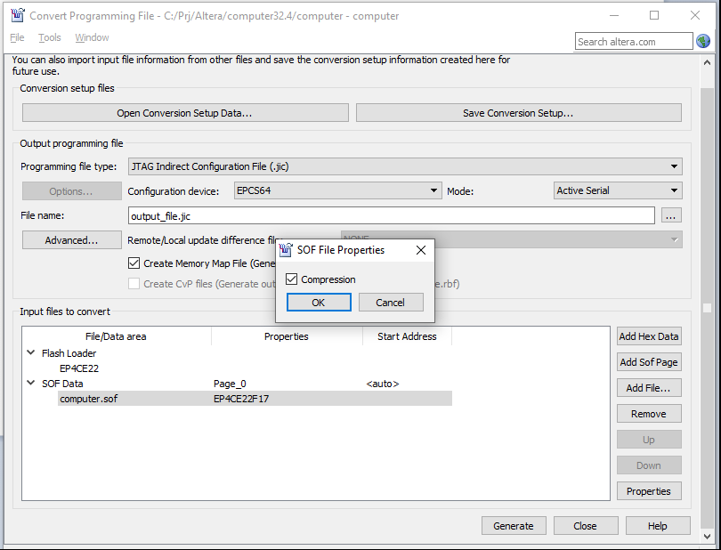
5. Click on the SOF Data in the table and click on the Add File... button. Choose your SOF file:

6. Click on the chosen SOF file in the table (in my example, the computer.sof file) and click on the Properties. Turn on the compression:
7. After that start the Programmer, delete the SOF file (if existed), and add the JIC file (click on the Add File... button). Make sure that both Program/Configure checkboxes are turned on:
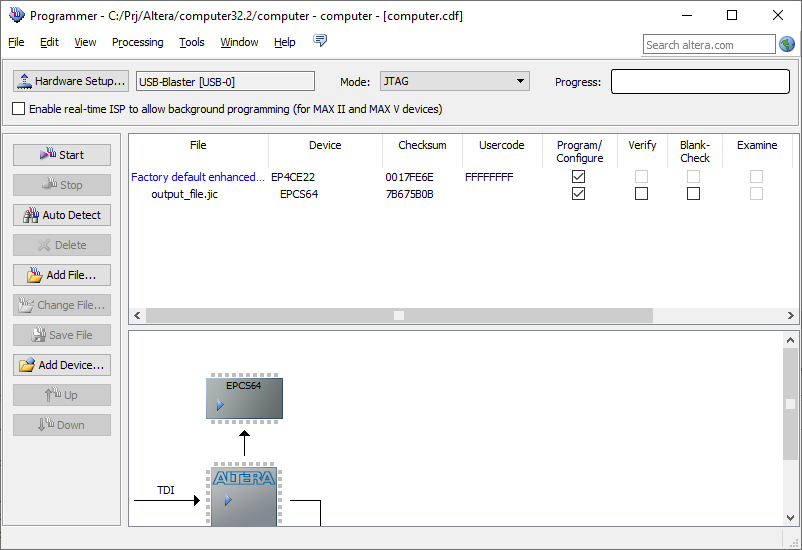
8. Click on the Start button and wait for the 100% at the progress bar (upper right corner).
9. You can power off and then power on the FPGA and it will still have the design in it.
Reset all registers with the Reset button (DEV_CLRn option)
I have experienced some strange behavior regarding resetting my design. I have made my KEY[0] clear all of my registers using the Verilog code. That design, however, failed somehow to completely reset my board. Simply, after the reset, the design would behave unreliable. I have managed to solve this problem by introducing the mega-reset feature. Here is the explanation:In DE0-NANO, the KEY[0] is connected to the PIN_J15, which is in turn connected to the DEV_CLRn pin. This can be used to reset all registers in the FPGA when you press the KEY[0] key on the DE0-NANO board. That is a kind of mega-reset. However, this feature is turned off by default. You need to enable it. Here is the procedure:
1. right click on the Cyclone IV... in the Project Navigator and choose the Device... option:

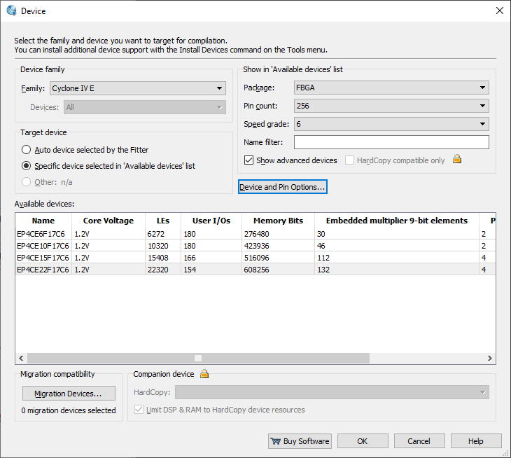
2. click on the Device and Pin Options... button:
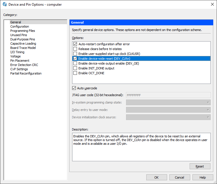
3. Find and enable the Enable device-wide reset (DEV_CLRn) check box:
4. Open the Pin Planner dialog (Assignments -> Pin Planner menu option), and change the KEY[0] from PIN_J15 to something unassigned, like PIN_G5 (it is unused in my project):

After that, whenever you press the KEY[0] key, you will reset your entire board.