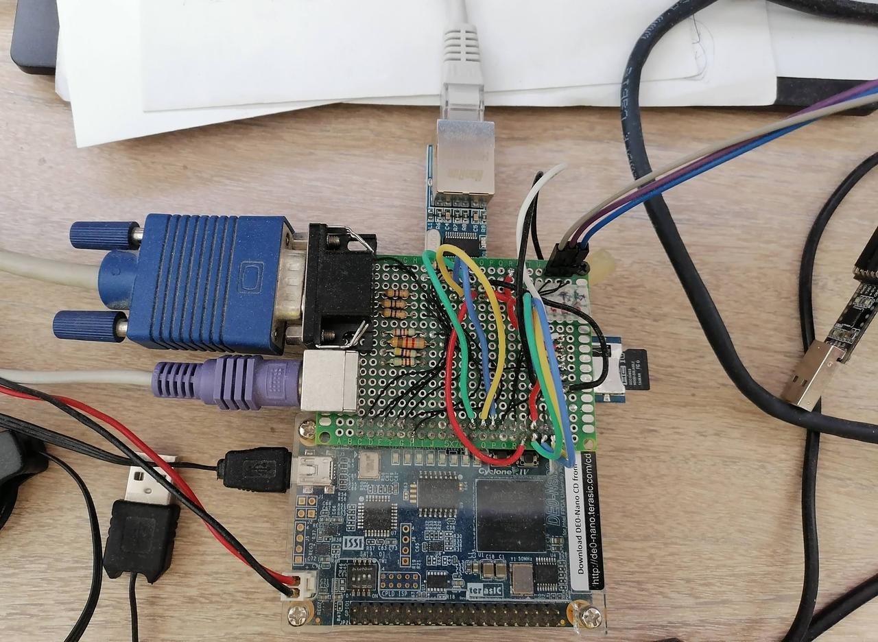
This is a followup of my original post.
I have recently implemented the BLIT instruction for my FPGA computer. It is the
most simple version of BLIT: copy the given number of bytes from the source memory location to the destination
memory location. The syntax is like this:
mov.w r1, 1024 # destination address is in
r1
mov.w r2, 9024 # source address is in r2
mov.w r3, 8000 # number of bytes is in r3
blit # copy bytes
Registers r1, r2 and r3 are hardcoded. Later I might make it more flexible.
Results are quite impressive. When I copy 32KB using memcpy (not using BLIT), it
takes approximately 100 milliseconds. When I use the BLIT instruction, it takes one millisecond!
How is BLIT implemented? Here is the Verilog code:
4'b1000: begin
// BLIT (r1, r2, r3) - r1 - dst; r2 - src; r3 - count
case (mc_count)
0: begin
addr <= regs[2] >> 1;
regs[2] <= regs[2] + 2;
regs[3] <= regs[3] - 2;
mc_count <= 1;
next_state <= EXECUTE;
state <= READ_DATA;
end
1: begin
addr <= regs[1] >> 1;
data_to_write <= data_r;
regs[1] <= regs[1] + 2;
next_state <= EXECUTE;
state <= WRITE_DATA;
if (regs[3] <= 0) begin
mc_count <= 2;
end
else
mc_count <= 0;
end
2: begin
state <= CHECK_IRQ;
pc <= pc + 2;
end
endcase
end
In the code above we see that the CPU starts memory read at the address pointed by
the r2 register in the first mc_count cycle. Then it obtains the word (two bytes) from memory and writes
them to the address pointed by the r1 register. Both r1 and r2 are incremented by two and the r3 register is
decremented by two; when it reaches zero, the instruction finishes.
Conclusion
The BLIT instruction does not execute in parallel with the CPU. It blocks the CPU
while executing. Even with this constraint, it is approximately hundred times faster then copying bytes across
the memory using the memcpy function. Therefore, it is worth using.