Snakes!
The first game on my FPGA platform
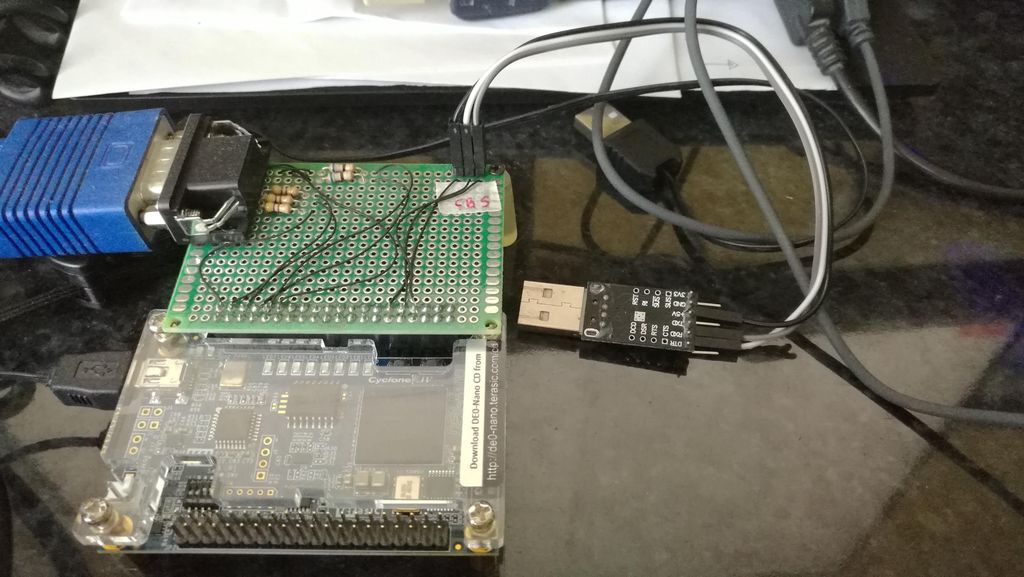
This is a follow-up of the FPGA computer post.
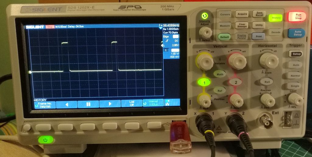
I have decided to make a game for the FPGA Computer. My friend gave me his Pascal implementation of the Snakes game and I have ported it into the FPGA Assembler. Not an easy task, but it works now:
I have decided to make a game for the FPGA Computer. My friend gave me his Pascal implementation of the Snakes game and I have ported it into the FPGA Assembler. Not an easy task, but it works now:

The game was made to work in the video text mode. The frame is constructed
using '-', '+', and '|' characters. The head of the snake is '@', the body is 'O', the star is '*', and when
the snake hits the wall or its tail, we get the 'X' character at the crash scene.
In the emulator it works the same way:

Milliseconds counter register
During the game development, it occured to me that I need to implement the
milliseconds counter register in order to implement the delay function. In the cpu.v
file, I have created two additional registers:
reg [N-1:0] millis_counter;
reg [15:0] clock_counter;
The millis_counter register will hold the number of milliseconds counted so far. Incrementing this
register is done whenever clock_counter reaches 50000 (clock is 50MHz, which means that when the
clock_counter reaches 50000, one millisecond has elapsed):
always @ (posedge CLOCK_50) begin
if (clock_counter < 50000) begin
clock_counter <= clock_counter + 1'b1;
end
else begin
clock_counter <= 0;
millis_counter <= millis_counter + 1'b1;
end
...
To read the millis_counter register, I have introduced another port address for the IN instruction:
4'b0011: begin
// IN reg, [xx]
`ifdef DEBUG
$display("%2x: IN r%-d, [%4d]",ir[3:0], (ir[11:8]), data);
`endif
case (mc_count)
0: begin
mbr <= data; // remember the address of IO
port
mc_count <= 1;
pc <= pc + 2'd2; // move to the next
instruction
end
1: begin
case (mbr)
64: begin // UART RX DATA
regs[ir[11:8]] <= {8'b0, rx_data_r};
end
65: begin // UART TX BUSY
regs[ir[11:8]] <= tx_busy;
end
68: begin // keyboard data
regs[ir[11:8]] <= {8'b0, ps2_data_r};
end
69: begin //
milliseconds counted so far
regs[ir[11:8]] <= millis_counter;
end
endcase // end of case(mbr)
ir <= 0; // initiate fetch
addr <= pc >> 1;
end
default: begin
end
endcase // end of case (mc_count)
end // end of IN reg, [xx]
The example of the usage can be found in the snakes.asm file:
; ################################################################
; function delay(r0)
; waits for the r0 milliseconds
; ################################################################
delay:
push r1
push r2
delay_loop2:
in r1, [PORT_MILLIS] ; port 69
delay_loop1:
in r2, [PORT_MILLIS] ; port 69
sub r2, r1
jz delay_loop1 ;
one millisecond elapsed here
dec r0
jnz delay_loop2
pop r2
pop r1
ret
Conclusion
This was the first game made for the FPGA Computer. The game is quite
simple and uses video text mode. I had to implement a milliseconds counter register and the
corresponding IN port to read it. It was used to implement the delay function.